共振結合型マイクロキャビティにおける低消費電力超広帯域ソリトンマイクロコム
The drive to miniaturize optical frequency combs for practical deployment has spotlighted microresonator solitons as a promising chip-scale candidate.
背景と学術的系譜
問題の起源と学術的系譜
本論文で取り上げられている問題の正確な起源は、高度な光周波数コムを専門的な実験室環境から実用的な応用へと移行させるという継続的な推進力に由来する。発明から約20年、光周波数コムは革命的なツールであったが、その広範な展開はサイズと消費電力によって妨げられてきた。したがって、集積フォトニクス分野はこれらのデバイスの小型化に焦点を当てており、有望なチップスケールソリューションとしてソリトンマイクロコムに注目が集まっている。
しかし、以前のアプローチにおける根本的な限界、すなわち「ペインポイント」が明らかになった。これらのチップスケールソリトンマイクロコムは、特に研究者がより広いスペクトル範囲(オクターブ広がりコムなど)や、多くの応用にとって重要な、より細かいコム間隔を目指す場合に、しばしば非常に多くの電力を消費した。本論文では、マイクロ波繰り返しレートでのオクターブ広がりコムを直接光マイクロ波リンクに利用することは、「高い電力要件のためフォトニック集積では不可能」と考えられていたと明記されている。非線形マイクロキャビティがバス導波路に直接結合される従来のアーキテクチャでは、四光波混合を開始するために入力ポンプ電力($P_{in}$)が特定のしきい値($P_{th}$)を超え、安定したソリトン形成のためにはさらに多くの電力が必要となる。これにより、コンパクトで電力効率が高く、広帯域なマイクロコムの実現を妨げる、重大な「ポンプ電力のボトルネック」が生じた。著者らは、このボトルネック、すなわち「不可能な三位一体」—限られたポンプ電力下で、特に帯域幅の増加や繰り返しレートの低下が極めて電力集約的になる二次スケーリング則のために、コムの帯域幅、電力、間隔を同時に最適化できないこと—を克服するために、本論文を執筆することを余儀なくされた。
従来の方式の根本的な限界は、著者らが「ソリトンマイクロコムの不可能な三位一体」(図1b)と呼ぶものに集約されている。
この概念は、限られたポンプ電力下では、コムのスペクトル帯域幅、出力電力、および繰り返しレートを同時に最適化することは不可能であることを強調している。
直感的ドメイン用語
- 光周波数コム (Optical Frequency Comb): 非常に精密な定規を想像してほしい。ただし、長さを測定するのではなく、光の周波数を測定する。この定規は、非常に安定した特定の周波数の光でできた、完全に均等に間隔が空いた「歯」(櫛のように)を持っている。これらの歯は基準点として機能し、科学者は他の光源を極めて正確に測定したり、非常に精密なタイミング信号を作成したりすることができる。
- ソリトンマイクロコム (Soliton Microcomb): 形状を変えずに海を渡る孤立した海の波のように、完全に安定した自己維持型の光の波を想像してほしい。次に、この光の波が、非常に効率的な小さな光学ループ(マイクロキャビティ)の中に閉じ込められ、循環していると想像してほしい。この安定性は、光自体の内部の力の繊細なバランスから生まれる。この安定した光の波が繰り返し生成されると、光周波数コムの「歯」が作成される。
- マイクロキャビティ (Microresonator): これは本質的に、光のための小型で高品質なトラックである。光はこの小さなリングまたはディスクに入り、何度も何度も循環し、その強度を増していく。「高Q」(高い品質係数)とは、光が各周回でほとんどエネルギーを失わないことを意味し、光と物質との強い相互作用を可能にし、コム生成に不可欠である。
- オクターブ広がり (Octave-spanning): 音楽では、オクターブは音符の周波数を倍にすることを意味する(例:中央のCから高いC)。光コムの文脈では、「オクターブ広がり」とは、コムがカバーする周波数範囲が、最も高い周波数が最も低い周波数の少なくとも2倍であることを意味する。この極めて広いカバレッジは、コム自体の絶対的な内蔵周波数標準を持つような自己参照などの高度な応用にとって不可欠である。
- 共振結合 (Resonant-coupling): これは、光供給システムにターボチャージャーを追加するようなものである。メインの「トラック」(非線形マイクロキャビティ)に直接光を注入するのではなく、まず、より小さく補助的な「ブースター」キャビティに送る。このブースターは、入力光と共振するように特別に調整されており、メインキャビティに効率的に転送される前に、ポンプ電力を効果的に増幅・集中させる。これにより、ソリトンマイクロコム生成プロセス全体が、より電力効率が高くなる。
記法表
| 記法 | 説明 | タイプ |
|---|---|---|
| $P_{in}$ | 入力ポンプ電力 | 変数 |
| $\Delta f_{3dB}$ | 光周波数コムの3dB帯域幅 | 変数 |
| $P_c$ | 光周波数コムの中心歯電力 | 変数 |
| $f_r$ | 光周波数コムの繰り返しレート | 変数 |
| $\delta\omega$ | ポンプ-非線形キャビティ(NR)デチューニング | 変数 |
| $\kappa_{NR}$ | 非線形キャビティ(NR)の全散逸率 | パラメータ |
| $\kappa_{RC}$ | 共振カプラ(RC)の全散逸率 | パラメータ |
| $G$ | 共振カプラ(RC)と非線形キャビティ(NR)間の結合率 | パラメータ |
| $\Gamma$ | 共振結合による実効ポンプ電力増強係数 | パラメータ |
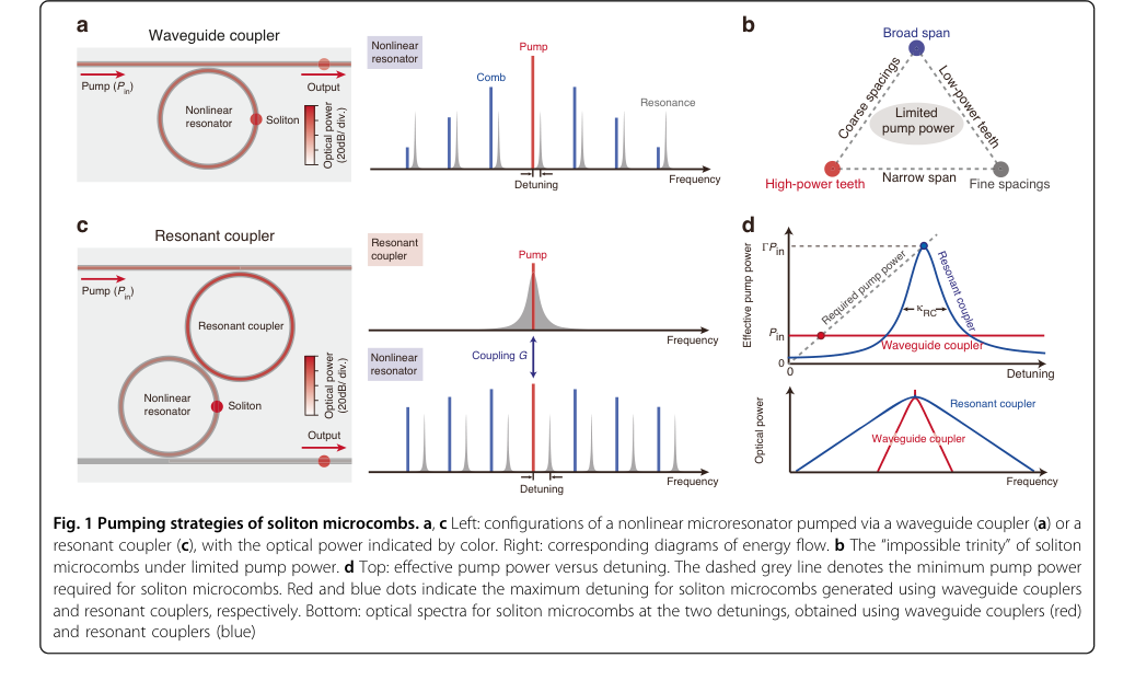 Figure 1. Pumping strategies of soliton microcombs. a, c Left: configurations of a nonlinear microresonator pumped via a waveguide coupler (a) or a resonant coupler (c), with the optical power indicated by color. Right: corresponding diagrams of energy flow. b The “impossible trinity” of soliton microcombs under limited pump power. d Top: effective pump power versus detuning. The dashed grey line denotes the minimum pump power required for soliton microcombs. Red and blue dots indicate the maximum detuning for soliton microcombs generated using waveguide couplers and resonant couplers, respectively. Bottom: optical spectra for soliton microcombs at the two detunings, obtained using waveguide couplers (red) and resonant couplers (blue)
問題定義と制約
コア問題の定式化とジレンマ
本論文で取り上げられている中心的な課題は、実用的でチップスケールな展開に適した低消費電力超広帯域ソリトンマイクロコムを生成する固有の困難さである。
入力/現状:
現在の状態は、連続波レーザーでポンピングされる高品質(高Q)非線形マイクロキャビティ(NR)内で生成される従来のソリトンマイクロコムである。これらのシステムは、ケアン非線形性と異常分散の繊細なバランスに依存して、位相コヒーレントなパルス列を生成する。これらのコムの主要な性能指標は、スペクトル帯域幅、個々のコム歯の電力、および繰り返しレート(歯の間隔)である。従来の導波路結合アーキテクチャでは、安定したソリトン形成には、入力ポンプ電力($P_{in}$)が特定のしきい値($P_{th}$)を超える必要があり、さらに赤色デチューニングされたポンプには追加の電力が必要となる。
望ましい終点/目標状態:
究極の目標は、オクターブ広がり(極めて広い帯域幅)のソリトンマイクロコムをマイクロ波繰り返しレートで、大幅に削減されたポンプ消費電力で達成することである。これにより、マイクロコムの小型化と広範な普及を妨げてきた「長年のポンプ電力のボトルネック」を克服することができる。このような電力効率が高くコンパクトなデバイスは、ポータブル光時計、大規模並列データリンク、およびフィールド展開可能な分光計などの応用にとって不可欠である。
欠落しているリンクと数学的ギャップ:
正確に欠落しているリンクは、非線形マイクロキャビティにポンプ電力を効率的に供給・増強し、それによってコム特性の望ましくないスケーリングに対処するメカニズムである。本論文は、これを「不可能な三位一体」と、従来のマイクロコムを支配する制約によって強調している。
$$ P_c \Delta f_{3dB}^2 / f_r < 3.1 \times \eta_{NR} P_{in} $$
ここで、$P_c$は中心歯電力、$\Delta f_{3dB}$は3dB帯域幅(スペクトルスパン)、$f_r$は繰り返しレート、$\eta_{NR}$はNRのローディングファクターである。この方程式は、より広い帯域幅($\Delta f_{3dB}$)またはより低い繰り返しレート($f_r$)を達成するためには、実質的に高いポンプ電力($P_{in}$)が必要であり、特に帯域幅に対して厳しい二次スケーリングがあることを明らかにする、重大な数学的ギャップを示している。この二次スケーリングは、非現実的な量のポンプ電力なしに、マイクロ波繰り返しレートでオクターブ広がりコムを達成することを極めて困難にしている。本論文は、NRに供給されるポンプ電力を効果的に増強する共振結合アーキテクチャを導入することによって、このギャップを埋めることを目指している。
ジレンマ(痛みを伴うトレードオフ):
著者らが「不可能な三位一体」(図1b)と呼ぶ中心的なジレンマは、3つの主要な性能指標—広いスペクトルスパン、高電力のコム歯、および細かいコム間隔—を同時に最適化することが、限られたポンプ電力下では極めて困難であるということである。
一方の側面を改善すると、通常はもう一方を劣化させるか、ポンプ電力の指数関数的な増加を要求する。例えば、従来のシステムでより広いスペクトルスパンまたはより細かいコム間隔(低い繰り返しレート)を達成するには、不釣り合いに多くのポンプ電力が必要となり、オクターブ広がりコムをマイクロ波レートで実現することは「高い電力要件のためフォトニック集積では不可能」となる。このトレードオフは、以前の研究者を閉じ込めてきた。なぜなら、帯域幅または繰り返しレートの限界を押し広げようとする試みは、すぐに法外な電力消費の壁に突き当たってしまうからである。
制約と故障モード
低消費電力、超広帯域ソリトンマイクロコムを生成する問題は、いくつかの厳しい現実的な制約のために非常に困難である。
-
極端なポンプ電力要件: 最も重大な制約は、広いスペクトルスパンと低い繰り返しレートを達成するために従来のマイクロコムに必要な高い光ポンプ電力である。二次スケーリング則(式1)で示されるように、帯域幅の増加または繰り返しレートの低下は、指数関数的に多くの電力を必要とする。例えば、本論文は、125mWおよび290mWのポンプ電力で共振カプラの性能に匹敵するためには、導波路結合デバイスではそれぞれ1.5Wおよび2Wを超える電力が必要になると推定している(図2h)。
これはチップスケール集積における主要な障壁である。
2. オンチップレーザー電力の制限: 小型化に不可欠な実用的なオンチップレーザーは、通常、限られた光出力を提供する。この基本的なハードウェアメモリ制限により、従来のマイクロコムの高いポンプ電力要件を満たすことが困難になり、ポータブルデバイスへの統合を防ぐ。
3. 複雑な分散管理: ソリトン形成は、ケアン非線形性と異常群速度分散(GVD)の正確なバランスに依存する。超広帯域、オクターブ広がりコムを達成するには、マイクロキャビティのGVDの慎重なエンジニアリングが必要となる。高次の分散やラマン自己周波数シフトなどの非線形効果は、達成可能な最大コムスパンを制限する可能性があり、慎重にバランスを取る必要があり、設計の複雑さを大幅に増す。
4. モード相互作用と不安定性:
* 回避モード交差: 特定のデチューニングでは、非線形キャビティ(NR)と共振カプラ(RC)のモード間の相互作用が「スペクトルスパー」とコムスペクトルの不規則性を引き起こす可能性がある(図2d)。より大きなデチューニングでこれを緩和できるが、他の問題を引き起こす。
* 変調不安定性: コムを広げるためにデチューニングを過度に大きくすると、共振カプラに変調不安定性が誘発され、それがソリトン自体を不安定化する。これは、アクセス可能な最大デチューニング、ひいては最大コムスパンに実用的な制限を設定する。
5. 製造精度と許容誤差: 共振結合アーキテクチャを実現するには、RCとNRの両方の物理的パラメータに対して極めて精密な制御が必要となる。これには、それらの固有および結合品質係数、ならびにそれらの相互キャビティ結合率が含まれる。所望の一般化臨界結合条件を達成し、バス導波路を介した直接的なポンプ伝送を最小限に抑えるには、Si3N4製造プロセスにおける厳しい製造許容誤差が必要となる。
6. 寄生効果と電力漏洩:
* 望ましくないパラメトリック発振: 共振カプラ自体が望ましくないパラメトリック発振を起こす可能性があり、これを抑制する必要がある(例:散逸率をエンジニアリングすることによって)。
* 寄生モード結合: ポンプされていない共振間の意図しない結合は、コム電力をNRからRCに漏洩させ、その後スルーポートから流出させる可能性があり、全体的な変換効率を低下させる。
7. ターンキー操作の課題: オンチップレーザーを使用した実用的な「ターンキー」操作では、自己注入ロック(後方散乱光がレーザーに再入射すること)などの現象がレーザーチューニングを摂動させる可能性がある。これは利用できるが、しばしば外部メカニズム(例:圧電ステージ)を介したフィードバック位相の正確な調整が必要であり、システムの複雑さを増し、堅牢性を低下させる。
Figure 1. Pumping strategies of soliton microcombs. a, c Left: configurations of a nonlinear microresonator pumped via a waveguide coupler (a) or a resonant coupler (c), with the optical power indicated by color. Right: corresponding diagrams of energy flow. b The “impossible trinity” of soliton microcombs under limited pump power. d Top: effective pump power versus detuning. The dashed grey line denotes the minimum pump power required for soliton microcombs. Red and blue dots indicate the maximum detuning for soliton microcombs generated using waveguide couplers and resonant couplers, respectively. Bottom: optical spectra for soliton microcombs at the two detunings, obtained using waveguide couplers (red) and resonant couplers (blue)
 Figure 2. High-power ultra-broadband soliton microcombs. a Photos of the wafer, chips, and the coupled Si3N4 microresonators. b Measured transmission spectra revealing the intrinsic quality factor Q0 and the external coupling quality factor Qe for both the resonant coupler and the nonlinear microresonator. c Transmission spectra from the through port as a function of the voltage (VRC) applied to the resonant coupler’s heater. The minimum frequency difference between the hybridized modes is 3.3 GHz. d–f Sequential stages for generating ultra-broadband solitons in a resonantly-coupled NR. Top panel: the relative frequency positions and tuning directions of the pump, RC, and NR. Bottom panel: corresponding optical spectra of soliton microcombs. g Comparison of optical spectra for soliton microcombs generated using conventional waveguide couplers (red) and resonant couplers (dark and light blue). All power refers to on-chip power. The pump powers on the bus waveguide, and the pump-to- comb conversion efficiencies are indicated. Communication bands covered by optical amplifiers are highlighted with different color shadings. h Measured minimum pump power as a function of 3 dB bandwidth of soliton microcombs pumped via the waveguide coupler (red dots) and the resonant coupler (blue dots) on a log-log scale. The red dashed line represents the quadratic scaling
なぜこのアプローチなのか
選択の必然性
共振結合型マイクロキャビティ(RC)アーキテクチャの採用は、単なる漸進的な改善ではなく、ソリトンマイクロコム技術における重要なボトルネックを克服するための根本的な必要性であった。著者らは、「マイクロ波繰り返しレートでのオクターブ広がりコムを直接光マイクロ波リンクに利用することは、高い電力要件のためフォトニック集積では不可能」であると明示的に特定している。この声明は、従来の導波路結合設計に依存した場合、従来の最先端(SOTA)手法が不十分であるという正確な瞬間の認識を示している。
従来の方式の根本的な限界は、著者らが「ソリトンマイクロコムの不可能な三位一体」(図1b)と呼ぶものに集約されている。
この概念は、限られたポンプ電力下では、コムのスペクトル帯域幅、出力電力、および繰り返しレートを同時に最適化することは不可能であることを強調している。支配的な方程式、$P_c \Delta f_{3dB}^2 / f_r < 3.1 \times \eta_{NR} P_{in}$(式9)は、二次スケーリング則を明確に示しており、帯域幅または繰り返しレートの増加が、単に歯の電力をブーストするよりも指数関数的に困難になることを示している。効率的なポンプ供給メカニズムを欠く従来の方式は、この電力集約的な性質によって根本的に制約されており、オクターブ広がり、低繰り返しレート、チップスケール集積という野心的な目標を達成不可能にしていた。RCアーキテクチャは、この電力ダイナミクスを根本的に変えることができる唯一の実行可能なソリューションとして登場した。
比較優位性
共振結合アプローチは、主にポンプ電力のボトルネックに対処することによって、以前のゴールドスタンダードに対して質的および構造的な利点を提供し、圧倒的に優れている。構造的には、この方法は補助的なマイクロキャビティ(RC)をバス導波路と非線形キャビティ(NR)の間に配置する。この一見単純な追加により、NRに供給されるポンプ電力の「共振増強」が提供され、増強係数 $\Gamma = 4G^2 / (K_{RC} K_{NR})$(式2)によって定量化される。
この共振増強は単なるマイナーなブーストではなく、ゲームチェンジャーである。これにより、システムは大幅に大きなデチューニング(図1d)にアクセスできるようになり、
それが「ソリトン帯域幅を劇的に増加させる」ことが可能になる。なぜなら、それは $\sqrt{\delta\omega}$ とスケーリングするからである。本論文は、従来の導波路結合設計と比較して、「高電力コムのスペクトル帯域幅の3倍の増加と、(ii)オクターブ広がり動作の繰り返し周波数の最大10倍の削減」を実証している。さらに驚くべきことに、RCアーキテクチャは、特定の帯域幅に対して「最大10倍のポンプ電力増強」(図2h)を達成している。
オクターブ広がりコム生成のためのフィギュア・オブ・メリット $P_{in} \times f_r^2$ を比較すると、RCアーキテクチャは $10^5 \text{ mW} \cdot \text{GHz}^2$ の値を示しており、これは「従来の導波路結合構成で報告された最高の結果よりも2桁低い」(図3f)ものである。
これは電力効率における根本的な質的飛躍を表しており、以前は不可能と考えられていたパフォーマンスを可能にする。
本論文では、典型的な機械学習アルゴリズムの文脈でメモリ複雑性や高次元ノイズ処理について議論していないが、生成されたコムの位相ノイズを特徴付けている(図3e)。結果は、自由走行型集積ソリトンマイクロコムで報告されている最低値に匹敵する位相ノイズを示しており、共振結合が有害なノイズ特性を導入せず、高いコヒーレンスを維持していることを示唆している。これは光時計などの応用にとって非常に重要である。主な優位性は、電力-帯域幅-繰り返しレートのトレードオフを破る能力にある。
制約との整合性
選択された共振結合法は、問題の厳格な制約と完全に整合しており、厳しい要件とソリューションのユニークな特性との真の「結婚」を形成している。
-
小型化とチップスケール展開: RCとNRの両方を含むアーキテクチャ全体がSi3N4チップ上に製造されており(図2a)、
コンパクトで統合されたソリューションの要求に直接応えている。
2. オクターブ広がり帯域幅: ポンプ電力の共振増強により、大幅に大きなデチューニングが可能になり、これは直接「劇的に増加したソリトン帯域幅」(図1d)に変換される。これにより、1007 nmから2130 nm(図3b)および1098 nmから2250 nm(図3d)の帯域幅を持つオクターブ広がりマイクロコムの生成が可能になる。
-
マイクロ波繰り返しレート: ポンプ電力のボトルネックを克服することにより、RCアーキテクチャは、100 GHzおよび25 GHz(図3b、d、e)などのマイクロ波領域の繰り返しレートを持つコムの生成を促進し、
これらは電子的に検出可能である。
4. 低ポンプ電力/電力効率: ここで整合性が最も顕著である。RCのポンプ供給を共振的に増強するというユニークな特性は、「長年のポンプ電力のボトルネック」に直接対処する。この方法は、同等の帯域幅に対して実質的に低いポンプ電力でオクターブ広がりコムを達成し、$P_{in} \times f_r^2$ フィギュア・オブ・メリット(図3f)において2桁の改善を示している。この主要な制約の直接的な緩和が「結婚」の本質である。
5. 信頼性の高いターンキーソリトン生成: 本論文は、「ハイブリッド集積型ターンキーソリトンマイクロコム」(図4)を実証している。自己注入ロックされたポンピングスキームにおけるフィードバック位相を最適化することにより、単一ソリトン状態は、「レーザー電流が所定の設定点に調整されるたびに決定論的に形成される」ことが示されており、堅牢で実用的な操作を保証している。
代替案の却下
本論文は、暗黙的かつ明示的に、従来の導波路結合マイクロキャビティ設計が、述べられた目標を達成するには不十分であると却下している。主な理由は、「不可能な三位一体」(図1b、式9)に起因しており、
これはこれらの従来の方式の性能を根本的に制限している。
著者らは、「マイクロ波繰り返しレートでのオクターブ広がりコムを直接光マイクロ波リンクに利用することは、高い電力要件のためフォトニック集積では不可能」であると強調している。これは、効率的なポンプ供給メカニズムなしに、広帯域、低繰り返しレートのコムを生成することの電力集約的な性質という根本的な物理的限界に基づいた直接的な却下である。
実験的ベンチマーキングは、この却下をさらに確固たるものにしている。図2hは、同一の幾何学的形状とQファクターを持つ導波路結合NRとRCアーキテクチャを直接比較している。
従来のデバイスは、600mWという高ポンプ電力でも7.2 THzの3dB帯域幅で頭打ちになる。対照的に、RCデバイスは、大幅に低いポンプ電力(125mWおよび290mW)で15.8 THzの帯域幅を達成している。導波路結合デバイスの二次スケーリングを外挿すると、「それぞれ125mWおよび290mWのポンプ電力でRCのパフォーマンスに匹敵するには、1.5Wおよび2Wを超える電力が必要になる」と示唆されている。この巨大な電力差は、従来の方式が低電力、オクターブ広がり要件を満たせない理由を強調している。
「不可能な三位一体」制約を緩和するための他の戦略(例:ファイバーまたは電気光学キャビティ内)が提案されているが、本論文は、オンチップ、連続波ポンピングソリトンマイクロコムにとって最も効果的で実用的なソリューションとして共振カプラを実証することに焦点を当てており、これらの他のアプローチは同じレベルのパフォーマンスを持っていないか、特定の集積プラットフォームと目標にはそれほど適していないことを示唆している。本論文では、GANや拡散などの代替案については議論していない。それらは光周波数コム生成とは全く異なるパラダイムであるためである。
Figure 1. Pumping strategies of soliton microcombs. a, c Left: configurations of a nonlinear microresonator pumped via a waveguide coupler (a) or a resonant coupler (c), with the optical power indicated by color. Right: corresponding diagrams of energy flow. b The “impossible trinity” of soliton microcombs under limited pump power. d Top: effective pump power versus detuning. The dashed grey line denotes the minimum pump power required for soliton microcombs. Red and blue dots indicate the maximum detuning for soliton microcombs generated using waveguide couplers and resonant couplers, respectively. Bottom: optical spectra for soliton microcombs at the two detunings, obtained using waveguide couplers (red) and resonant couplers (blue)
Figure 1. Pumping strategies of soliton microcombs. a, c Left: configurations of a nonlinear microresonator pumped via a waveguide coupler (a) or a resonant coupler (c), with the optical power indicated by color. Right: corresponding diagrams of energy flow. b The “impossible trinity” of soliton microcombs under limited pump power. d Top: effective pump power versus detuning. The dashed grey line denotes the minimum pump power required for soliton microcombs. Red and blue dots indicate the maximum detuning for soliton microcombs generated using waveguide couplers and resonant couplers, respectively. Bottom: optical spectra for soliton microcombs at the two detunings, obtained using waveguide couplers (red) and resonant couplers (blue)
Figure 2. High-power ultra-broadband soliton microcombs. a Photos of the wafer, chips, and the coupled Si3N4 microresonators. b Measured transmission spectra revealing the intrinsic quality factor Q0 and the external coupling quality factor Qe for both the resonant coupler and the nonlinear microresonator. c Transmission spectra from the through port as a function of the voltage (VRC) applied to the resonant coupler’s heater. The minimum frequency difference between the hybridized modes is 3.3 GHz. d–f Sequential stages for generating ultra-broadband solitons in a resonantly-coupled NR. Top panel: the relative frequency positions and tuning directions of the pump, RC, and NR. Bottom panel: corresponding optical spectra of soliton microcombs. g Comparison of optical spectra for soliton microcombs generated using conventional waveguide couplers (red) and resonant couplers (dark and light blue). All power refers to on-chip power. The pump powers on the bus waveguide, and the pump-to- comb conversion efficiencies are indicated. Communication bands covered by optical amplifiers are highlighted with different color shadings. h Measured minimum pump power as a function of 3 dB bandwidth of soliton microcombs pumped via the waveguide coupler (red dots) and the resonant coupler (blue dots) on a log-log scale. The red dashed line represents the quadratic scaling
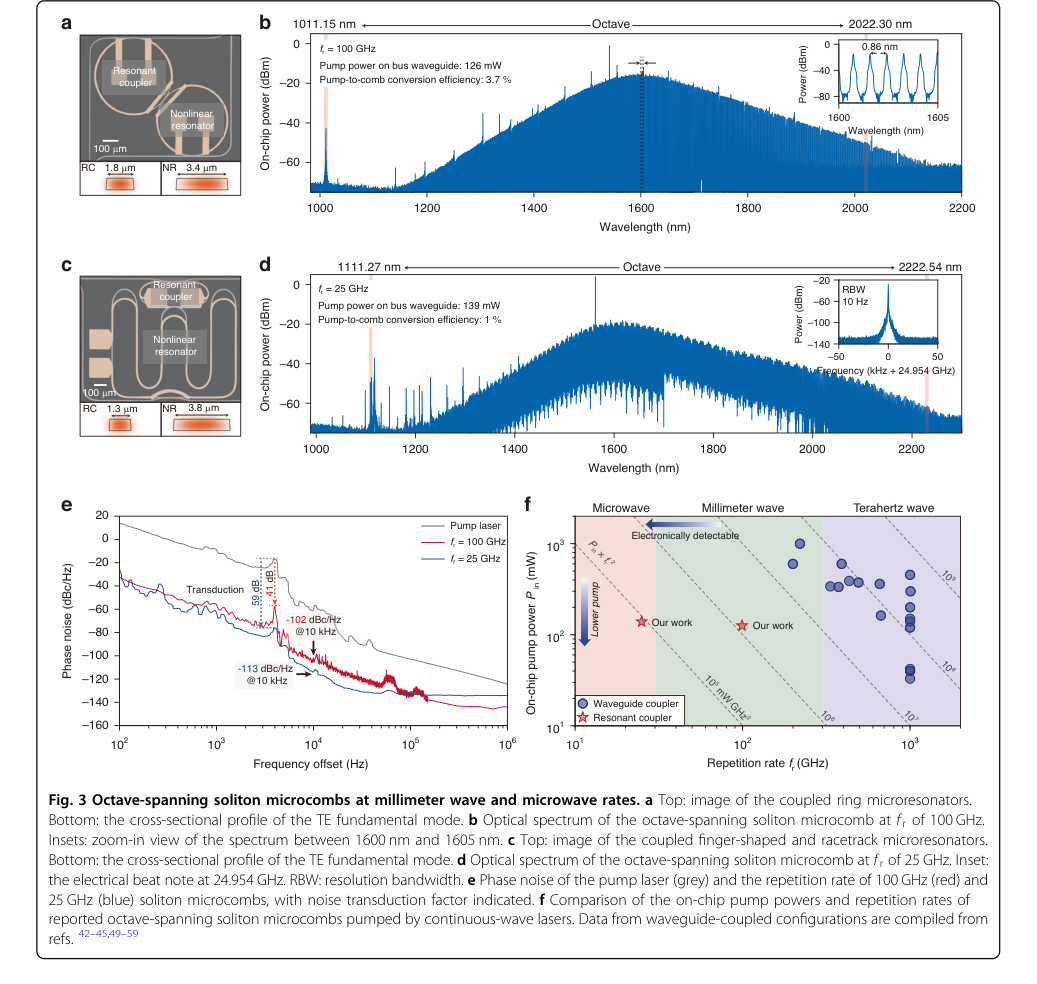 Figure 3. Octave-spanning soliton microcombs at millimeter wave and microwave rates. a Top: image of the coupled ring microresonators. Bottom: the cross-sectional profile of the TE fundamental mode. b Optical spectrum of the octave-spanning soliton microcomb at f r of 100 GHz. Insets: zoom-in view of the spectrum between 1600 nm and 1605 nm. c Top: image of the coupled finger-shaped and racetrack microresonators. Bottom: the cross-sectional profile of the TE fundamental mode. d Optical spectrum of the octave-spanning soliton microcomb at f r of 25 GHz. Inset: the electrical beat note at 24.954 GHz. RBW: resolution bandwidth. e Phase noise of the pump laser (grey) and the repetition rate of 100 GHz (red) and 25 GHz (blue) soliton microcombs, with noise transduction factor indicated. f Comparison of the on-chip pump powers and repetition rates of reported octave-spanning soliton microcombs pumped by continuous-wave lasers. Data from waveguide-coupled configurations are compiled from refs. 42–45,49–59
Figure 2. High-power ultra-broadband soliton microcombs. a Photos of the wafer, chips, and the coupled Si3N4 microresonators. b Measured transmission spectra revealing the intrinsic quality factor Q0 and the external coupling quality factor Qe for both the resonant coupler and the nonlinear microresonator. c Transmission spectra from the through port as a function of the voltage (VRC) applied to the resonant coupler’s heater. The minimum frequency difference between the hybridized modes is 3.3 GHz. d–f Sequential stages for generating ultra-broadband solitons in a resonantly-coupled NR. Top panel: the relative frequency positions and tuning directions of the pump, RC, and NR. Bottom panel: corresponding optical spectra of soliton microcombs. g Comparison of optical spectra for soliton microcombs generated using conventional waveguide couplers (red) and resonant couplers (dark and light blue). All power refers to on-chip power. The pump powers on the bus waveguide, and the pump-to- comb conversion efficiencies are indicated. Communication bands covered by optical amplifiers are highlighted with different color shadings. h Measured minimum pump power as a function of 3 dB bandwidth of soliton microcombs pumped via the waveguide coupler (red dots) and the resonant coupler (blue dots) on a log-log scale. The red dashed line represents the quadratic scaling
Figure 1. Pumping strategies of soliton microcombs. a, c Left: configurations of a nonlinear microresonator pumped via a waveguide coupler (a) or a resonant coupler (c), with the optical power indicated by color. Right: corresponding diagrams of energy flow. b The “impossible trinity” of soliton microcombs under limited pump power. d Top: effective pump power versus detuning. The dashed grey line denotes the minimum pump power required for soliton microcombs. Red and blue dots indicate the maximum detuning for soliton microcombs generated using waveguide couplers and resonant couplers, respectively. Bottom: optical spectra for soliton microcombs at the two detunings, obtained using waveguide couplers (red) and resonant couplers (blue)
Figure 3. Octave-spanning soliton microcombs at millimeter wave and microwave rates. a Top: image of the coupled ring microresonators. Bottom: the cross-sectional profile of the TE fundamental mode. b Optical spectrum of the octave-spanning soliton microcomb at f r of 100 GHz. Insets: zoom-in view of the spectrum between 1600 nm and 1605 nm. c Top: image of the coupled finger-shaped and racetrack microresonators. Bottom: the cross-sectional profile of the TE fundamental mode. d Optical spectrum of the octave-spanning soliton microcomb at f r of 25 GHz. Inset: the electrical beat note at 24.954 GHz. RBW: resolution bandwidth. e Phase noise of the pump laser (grey) and the repetition rate of 100 GHz (red) and 25 GHz (blue) soliton microcombs, with noise transduction factor indicated. f Comparison of the on-chip pump powers and repetition rates of reported octave-spanning soliton microcombs pumped by continuous-wave lasers. Data from waveguide-coupled configurations are compiled from refs. 42–45,49–59
Figure 3. Octave-spanning soliton microcombs at millimeter wave and microwave rates. a Top: image of the coupled ring microresonators. Bottom: the cross-sectional profile of the TE fundamental mode. b Optical spectrum of the octave-spanning soliton microcomb at f r of 100 GHz. Insets: zoom-in view of the spectrum between 1600 nm and 1605 nm. c Top: image of the coupled finger-shaped and racetrack microresonators. Bottom: the cross-sectional profile of the TE fundamental mode. d Optical spectrum of the octave-spanning soliton microcomb at f r of 25 GHz. Inset: the electrical beat note at 24.954 GHz. RBW: resolution bandwidth. e Phase noise of the pump laser (grey) and the repetition rate of 100 GHz (red) and 25 GHz (blue) soliton microcombs, with noise transduction factor indicated. f Comparison of the on-chip pump powers and repetition rates of reported octave-spanning soliton microcombs pumped by continuous-wave lasers. Data from waveguide-coupled configurations are compiled from refs. 42–45,49–59
Figure 3. Octave-spanning soliton microcombs at millimeter wave and microwave rates. a Top: image of the coupled ring microresonators. Bottom: the cross-sectional profile of the TE fundamental mode. b Optical spectrum of the octave-spanning soliton microcomb at f r of 100 GHz. Insets: zoom-in view of the spectrum between 1600 nm and 1605 nm. c Top: image of the coupled finger-shaped and racetrack microresonators. Bottom: the cross-sectional profile of the TE fundamental mode. d Optical spectrum of the octave-spanning soliton microcomb at f r of 25 GHz. Inset: the electrical beat note at 24.954 GHz. RBW: resolution bandwidth. e Phase noise of the pump laser (grey) and the repetition rate of 100 GHz (red) and 25 GHz (blue) soliton microcombs, with noise transduction factor indicated. f Comparison of the on-chip pump powers and repetition rates of reported octave-spanning soliton microcombs pumped by continuous-wave lasers. Data from waveguide-coupled configurations are compiled from refs. 42–45,49–59
Figure 1. Pumping strategies of soliton microcombs. a, c Left: configurations of a nonlinear microresonator pumped via a waveguide coupler (a) or a resonant coupler (c), with the optical power indicated by color. Right: corresponding diagrams of energy flow. b The “impossible trinity” of soliton microcombs under limited pump power. d Top: effective pump power versus detuning. The dashed grey line denotes the minimum pump power required for soliton microcombs. Red and blue dots indicate the maximum detuning for soliton microcombs generated using waveguide couplers and resonant couplers, respectively. Bottom: optical spectra for soliton microcombs at the two detunings, obtained using waveguide couplers (red) and resonant couplers (blue)
Figure 2. High-power ultra-broadband soliton microcombs. a Photos of the wafer, chips, and the coupled Si3N4 microresonators. b Measured transmission spectra revealing the intrinsic quality factor Q0 and the external coupling quality factor Qe for both the resonant coupler and the nonlinear microresonator. c Transmission spectra from the through port as a function of the voltage (VRC) applied to the resonant coupler’s heater. The minimum frequency difference between the hybridized modes is 3.3 GHz. d–f Sequential stages for generating ultra-broadband solitons in a resonantly-coupled NR. Top panel: the relative frequency positions and tuning directions of the pump, RC, and NR. Bottom panel: corresponding optical spectra of soliton microcombs. g Comparison of optical spectra for soliton microcombs generated using conventional waveguide couplers (red) and resonant couplers (dark and light blue). All power refers to on-chip power. The pump powers on the bus waveguide, and the pump-to- comb conversion efficiencies are indicated. Communication bands covered by optical amplifiers are highlighted with different color shadings. h Measured minimum pump power as a function of 3 dB bandwidth of soliton microcombs pumped via the waveguide coupler (red dots) and the resonant coupler (blue dots) on a log-log scale. The red dashed line represents the quadratic scaling
Figure 3. Octave-spanning soliton microcombs at millimeter wave and microwave rates. a Top: image of the coupled ring microresonators. Bottom: the cross-sectional profile of the TE fundamental mode. b Optical spectrum of the octave-spanning soliton microcomb at f r of 100 GHz. Insets: zoom-in view of the spectrum between 1600 nm and 1605 nm. c Top: image of the coupled finger-shaped and racetrack microresonators. Bottom: the cross-sectional profile of the TE fundamental mode. d Optical spectrum of the octave-spanning soliton microcomb at f r of 25 GHz. Inset: the electrical beat note at 24.954 GHz. RBW: resolution bandwidth. e Phase noise of the pump laser (grey) and the repetition rate of 100 GHz (red) and 25 GHz (blue) soliton microcombs, with noise transduction factor indicated. f Comparison of the on-chip pump powers and repetition rates of reported octave-spanning soliton microcombs pumped by continuous-wave lasers. Data from waveguide-coupled configurations are compiled from refs. 42–45,49–59
Figure 2. High-power ultra-broadband soliton microcombs. a Photos of the wafer, chips, and the coupled Si3N4 microresonators. b Measured transmission spectra revealing the intrinsic quality factor Q0 and the external coupling quality factor Qe for both the resonant coupler and the nonlinear microresonator. c Transmission spectra from the through port as a function of the voltage (VRC) applied to the resonant coupler’s heater. The minimum frequency difference between the hybridized modes is 3.3 GHz. d–f Sequential stages for generating ultra-broadband solitons in a resonantly-coupled NR. Top panel: the relative frequency positions and tuning directions of the pump, RC, and NR. Bottom panel: corresponding optical spectra of soliton microcombs. g Comparison of optical spectra for soliton microcombs generated using conventional waveguide couplers (red) and resonant couplers (dark and light blue). All power refers to on-chip power. The pump powers on the bus waveguide, and the pump-to- comb conversion efficiencies are indicated. Communication bands covered by optical amplifiers are highlighted with different color shadings. h Measured minimum pump power as a function of 3 dB bandwidth of soliton microcombs pumped via the waveguide coupler (red dots) and the resonant coupler (blue dots) on a log-log scale. The red dashed line represents the quadratic scaling
Figure 1. Pumping strategies of soliton microcombs. a, c Left: configurations of a nonlinear microresonator pumped via a waveguide coupler (a) or a resonant coupler (c), with the optical power indicated by color. Right: corresponding diagrams of energy flow. b The “impossible trinity” of soliton microcombs under limited pump power. d Top: effective pump power versus detuning. The dashed grey line denotes the minimum pump power required for soliton microcombs. Red and blue dots indicate the maximum detuning for soliton microcombs generated using waveguide couplers and resonant couplers, respectively. Bottom: optical spectra for soliton microcombs at the two detunings, obtained using waveguide couplers (red) and resonant couplers (blue)
Figure 3. Octave-spanning soliton microcombs at millimeter wave and microwave rates. a Top: image of the coupled ring microresonators. Bottom: the cross-sectional profile of the TE fundamental mode. b Optical spectrum of the octave-spanning soliton microcomb at f r of 100 GHz. Insets: zoom-in view of the spectrum between 1600 nm and 1605 nm. c Top: image of the coupled finger-shaped and racetrack microresonators. Bottom: the cross-sectional profile of the TE fundamental mode. d Optical spectrum of the octave-spanning soliton microcomb at f r of 25 GHz. Inset: the electrical beat note at 24.954 GHz. RBW: resolution bandwidth. e Phase noise of the pump laser (grey) and the repetition rate of 100 GHz (red) and 25 GHz (blue) soliton microcombs, with noise transduction factor indicated. f Comparison of the on-chip pump powers and repetition rates of reported octave-spanning soliton microcombs pumped by continuous-wave lasers. Data from waveguide-coupled configurations are compiled from refs. 42–45,49–59
Figure 3. Octave-spanning soliton microcombs at millimeter wave and microwave rates. a Top: image of the coupled ring microresonators. Bottom: the cross-sectional profile of the TE fundamental mode. b Optical spectrum of the octave-spanning soliton microcomb at f r of 100 GHz. Insets: zoom-in view of the spectrum between 1600 nm and 1605 nm. c Top: image of the coupled finger-shaped and racetrack microresonators. Bottom: the cross-sectional profile of the TE fundamental mode. d Optical spectrum of the octave-spanning soliton microcomb at f r of 25 GHz. Inset: the electrical beat note at 24.954 GHz. RBW: resolution bandwidth. e Phase noise of the pump laser (grey) and the repetition rate of 100 GHz (red) and 25 GHz (blue) soliton microcombs, with noise transduction factor indicated. f Comparison of the on-chip pump powers and repetition rates of reported octave-spanning soliton microcombs pumped by continuous-wave lasers. Data from waveguide-coupled configurations are compiled from refs. 42–45,49–59
Figure 3. Octave-spanning soliton microcombs at millimeter wave and microwave rates. a Top: image of the coupled ring microresonators. Bottom: the cross-sectional profile of the TE fundamental mode. b Optical spectrum of the octave-spanning soliton microcomb at f r of 100 GHz. Insets: zoom-in view of the spectrum between 1600 nm and 1605 nm. c Top: image of the coupled finger-shaped and racetrack microresonators. Bottom: the cross-sectional profile of the TE fundamental mode. d Optical spectrum of the octave-spanning soliton microcomb at f r of 25 GHz. Inset: the electrical beat note at 24.954 GHz. RBW: resolution bandwidth. e Phase noise of the pump laser (grey) and the repetition rate of 100 GHz (red) and 25 GHz (blue) soliton microcombs, with noise transduction factor indicated. f Comparison of the on-chip pump powers and repetition rates of reported octave-spanning soliton microcombs pumped by continuous-wave lasers. Data from waveguide-coupled configurations are compiled from refs. 42–45,49–59
Figure 1. Pumping strategies of soliton microcombs. a, c Left: configurations of a nonlinear microresonator pumped via a waveguide coupler (a) or a resonant coupler (c), with the optical power indicated by color. Right: corresponding diagrams of energy flow. b The “impossible trinity” of soliton microcombs under limited pump power. d Top: effective pump power versus detuning. The dashed grey line denotes the minimum pump power required for soliton microcombs. Red and blue dots indicate the maximum detuning for soliton microcombs generated using waveguide couplers and resonant couplers, respectively. Bottom: optical spectra for soliton microcombs at the two detunings, obtained using waveguide couplers (red) and resonant couplers (blue)
Figure 2. High-power ultra-broadband soliton microcombs. a Photos of the wafer, chips, and the coupled Si3N4 microresonators. b Measured transmission spectra revealing the intrinsic quality factor Q0 and the external coupling quality factor Qe for both the resonant coupler and the nonlinear microresonator. c Transmission spectra from the through port as a function of the voltage (VRC) applied to the resonant coupler’s heater. The minimum frequency difference between the hybridized modes is 3.3 GHz. d–f Sequential stages for generating ultra-broadband solitons in a resonantly-coupled NR. Top panel: the relative frequency positions and tuning directions of the pump, RC, and NR. Bottom panel: corresponding optical spectra of soliton microcombs. g Comparison of optical spectra for soliton microcombs generated using conventional waveguide couplers (red) and resonant couplers (dark and light blue). All power refers to on-chip power. The pump powers on the bus waveguide, and the pump-to- comb conversion efficiencies are indicated. Communication bands covered by optical amplifiers are highlighted with different color shadings. h Measured minimum pump power as a function of 3 dB bandwidth of soliton microcombs pumped via the waveguide coupler (red dots) and the resonant coupler (blue dots) on a log-log scale. The red dashed line represents the quadratic scaling
数学的・論理的メカニズム
マスター方程式
非線形マイクロキャビティ(NR)内での光ソリトンの形成と進化を支配する基本的なダイナミクスは、ルジアート・レフェバー方程式(LLE)によって記述される。この偏微分方程式は、光増幅、損失、分散、および非線形性の相互作用を捉えており、これらはマイクロコム生成に不可欠な要素である。本論文のソリトンマイクロコムの基礎物理学を支える絶対的なコア方程式は次のとおりである。
$$ \frac{\partial A}{\partial T} = -\frac{\kappa_{NR}}{2} A - i\delta\omega A + i\frac{D_2}{2}\frac{\partial^2 A}{\partial\phi^2} + ig|A|^2A + \sqrt{\frac{\kappa_{e,NR}P_{in}}{\hbar\omega_0}} $$
項ごとの解剖
このマスター方程式の各成分を詳細に分析し、その数学的定義、物理的役割、および著者による演算子の選択を理解しよう。
-
$\frac{\partial A}{\partial T}$:
- 数学的定義: これは、複素場振幅 $A$ の遅延時間 $T$ に対する偏微分である。
- 物理的/論理的役割: この項は、マイクロキャビティ内の光場の時間的進化を表す。それは、場の振幅と位相が時間とともにどのように変化するかを決定し、システム全体のダイナミクスを定常状態またはソリトン解へと駆動する。偏微分の使用は、場が空間的依存性(リングの円周に沿って)も持つことを意味する。
- なぜ偏微分か: 場 $A$ は時間 $T$ と角度座標 $\phi$ の両方の関数である。その進化を、空間プロファイルを考慮しながら記述するには偏微分が必要である。
-
$A$:
- 数学的定義: マイクロキャビティ内を循環する光場の遅延複素振幅。 $|A|^2$ が、腔内光子数に対応するように正規化されている。
- 物理的/論理的役割: この変数は、光場自体を記述する中心的な量である。その大きさの二乗は、特定の共振器内の瞬時光パワーまたは光子数を与える。
-
$T$:
- 数学的定義: 「遅延時間」または実験室時間。
- 物理的/論理的役割: これは、光場のエンベロープが進化する巨視的な時間スケールを表す。これは、はるかに速い光振動周期とは異なる。
-
$\phi$:
- 数学的定義: 循環する光パルスとともに移動する参照フレームにおける角度座標。
- 物理的/論理的役割: この空間座標は、マイクロキャビティの円周上の位置を表す。移動フレームを使用することにより、方程式は、光パルス(ソリトン)がリングの周りを移動する際の形状と伝播を効果的に記述できる。
-
$-\frac{\kappa_{NR}}{2} A$:
- 数学的定義: 場 $A$ に比例する線形減衰項。 $\kappa_{NR}$ は非線形キャビティの全減衰率である。
- 物理的/論理的役割: この項は、マイクロキャビティ内のすべての光損失を考慮する。これには、固有損失(物質吸収と散乱による)と、光が導波路からキャビティを脱出する際の結合損失が含まれる。これは減衰力として作用し、腔内場を継続的に減少させる。
- なぜ減算か: 損失を表すため、場の振幅を減少させる。
- $\kappa_{NR}$: 全減衰率であり、$\kappa_{NR} = \kappa_{0,NR} + \kappa_{e,NR}$ と定義される。ここで、$\kappa_{0,NR}$ は固有(内部)減衰率、$\kappa_{e,NR}$ は導波路への外部結合率である。
-
$-i\delta\omega A$:
- 数学的定義: $A$ に比例し、虚数単位 $i$ で乗算されたデチューニング項。 $\delta\omega$ はポンプ-NRデチューニングである。
- 物理的/論理的役割: この項は、ポンプレーザーとマイクロキャビティの光共振との間の周波数ずれを表す。正の $\delta\omega$ は、ポンプが共振よりも高い周波数(青色デチューニング)にあることを意味し、負の $\delta\omega$ は、それが低い周波数(赤色デチューニング)にあることを意味する。この項は、循環場に位相シフトを誘発し、通常は赤色デチューニングを必要とする安定したソリトン形成に重要である。
- なぜ虚数単位 $i$ か: これは、この項が主に場の振幅の変化ではなく、位相シフトを引き起こすことを示している。
-
$i\frac{D_2}{2}\frac{\partial^2 A}{\partial\phi^2}$:
- 数学的定義: $A$ の $\phi$ に対する2次偏微分を含む2次分散項。 $D_2$ は2次群速度分散(GVD)である。
- 物理的/論理的役割: この項は、光パルスの異なる周波数成分がキャビティ内で異なる速度で伝播することを記述する。 $D_2 < 0$ (異常分散)の場合、高周波は遅く伝播し、これはケアン非線形性とバランスをとって明るいソリトンを形成するために不可欠である。この項は、光パルスを広げたり圧縮したりする。
- なぜ虚数単位 $i$ か: 分散は主に周波数成分間の位相関係に影響を与え、パルス整形につながる。
- なぜ2次微分か: 群速度の周波数依存性を記述する最低次の項であり、パルス伝播に不可欠である。
-
$ig|A|^2A$:
- 数学的定義: ケアン非線形項であり、$|A|^2A$ に比例し、$i$ で乗算されている。 $g$ は非線形係数である。
- 物理的/論理的役割: この項は、自己位相変調(SPM)効果を表す。物質の屈折率は光の強度($|A|^2$)とともに変化し、強度依存の位相シフトを引き起こす。この効果は、異常分散とバランスをとってソリトンを形成できる。
- なぜ虚数単位 $i$ か: ケアン非線形性は、主に場の振幅変化ではなく、位相シフトを誘発する。
- $g$: 非線形係数であり、$g = \frac{\hbar\omega_0 c n_2}{n_{eff}^2 V_{eff}}$ と定義される。ここで、$\hbar\omega_0$ は光子エネルギー、 $c$ は光速、 $n_2$ は非線形屈折率、 $n_{eff}$ は実効屈折率、 $V_{eff}$ は実効モード体積である。
-
$\sqrt{\frac{\kappa_{e,NR}P_{in}}{\hbar\omega_0}}$:
- 数学的定義: 共振器のコヒーレントな駆動を表すコヒーレントポンプ項。
- 物理的/論理的役割: この項は、外部ポンプレーザーからマイクロキャビティに連続的に光パワーを注入する。これはシステムのエネルギー源として機能し、損失を相殺し、四光波混合とソリトン形成に必要な電力を提供する。
- なぜ平方根か: 場 $A$ は光パワーの平方根に比例する。
- $\kappa_{e,NR}$: バス導波路から非線形キャビティへの結合率。
- $P_{in}$: 入力ポンプ電力。共振カプラ(RC)アーキテクチャの場合、この $P_{in}$ は実質的に $\Gamma = \frac{4G^2}{\kappa_{RC}\kappa_{NR}}$(式2より)の係数で増強されるため、NRに供給される実際の電力は $\Gamma P_{in}$ となる。
- $\hbar\omega_0$: ポンプ周波数における単一光子のエネルギー。
ステップバイステップフロー
ここでは、抽象的な光「データポイント」(光子パケット)がこの数学的エンジンと相互作用する際の旅を追跡し、特に共振カプラの役割を強調する。
- 外部ポンプ注入: 特定の周波数 $\omega_0$ で電力 $P_{in}$ の連続波レーザーが光を発する。この光がシステムに入る初期「データポイント」である。
- 共振カプラ(RC)増強: 共振カプラアーキテクチャが採用されている場合、このポンプ光はまず補助的な共振カプラに入る。RCはポンプ周波数と共振するように精密に調整されており、メイン非線形キャビティ(NR)に到達する前に、RC内の光パワーの大幅な蓄積を引き起こす。これにより、NRに供給される実効ポンプ電力が効果的に増幅される。増強係数 $\Gamma$(式2より)はこのブーストを定量化し、NRに供給される実効ポンプ電力が $\Gamma P_{in}$ であることを意味する。従来の導波路結合システムでは、このステップはバイパスされ、$P_{in}$ が直接NRに結合される。
- 非線形キャビティ(NR)へのエネルギー供給: (増強された可能性のある)ポンプ電力は、次に非線形マイクロキャビティに結合される。このエネルギーの連続的な注入は、LLEの $\sqrt{\frac{\kappa_{e,NR}P_{in}}{\hbar\omega_0}}$ 項によって表され、腔内場 $A$ の定数駆動源として機能する。
- 循環と損失: NR内に入ると、光場 $A$ は循環する。伝播するにつれて、そのエネルギーの一部は、固有の物質吸収、散乱、およびキャビティからの結合により、継続的に失われる。この減衰は $-\frac{\kappa_{NR}}{2} A$ 項によってモデル化され、場を減少させるように作用する。
- デチューニング誘発位相進化: ポンプレーザーの周波数は、意図的にNRの自然周波数から $\delta\omega$ だけわずかにオフ共振に設定されている。このデチューニング($-i\delta\omega A$ 項で表される)は、循環場に連続的な位相シフトを引き起こす。安定したソリトン形成のためには、通常、特定の量の「赤色デチューニング」(ポンプ周波数が共振周波数より低い)が必要である。
- 分散誘発パルス広がり/圧縮: 光場がリングの周りを伝播するにつれて、その異なる周波数成分は、物質の群速度分散($D_2$)のために、わずかに異なる速度で伝播する。 $i\frac{D_2}{2}\frac{\partial^2 A}{\partial\phi^2}$ 項は、この分散がパルスをどのように整形するかを記述する。明るいソリトンの場合、異常分散($D_2 < 0$)はパルスを圧縮させ、そうでなければ発生する広がりを相殺する。
- ケアン非線形誘発自己位相変調: 循環光自体の高強度は、マイクロキャビティ物質の屈折率(ケアン効果)を変化させる。この強度依存の屈折率は、光強度に比例する位相シフトを引き起こし、$ig|A|^2A$ 項によって記述される。この「自己位相変調」(SPM)は、光パルスのピークで、その翼よりも強い。
- 動的バランスとソリトン形成: システムは継続的に進化し、$\frac{\partial A}{\partial T}$ 項はこれらのすべてのプロセスの正味の効果を反映する。ポンプ電力、デチューニング、分散、および非線形性が正確にバランスが取れている場合、分散広がりはケアン非線形性の自己焦点化様効果によって正確に補償される。この繊細なバランスにより、形状を変えずに循環する安定した自己維持型の光パルス—ソリトン—の形成が可能になる。これらのソリトンは、時間領域ではパルストレインとして、スペクトル領域では周波数コムとして現れる。
- 出力と測定: 循環ソリトン場の大部分は、キャビティから連続的に結合され($\kappa_{e,NR}$ の一部)、マイクロコム出力として検出可能になり、様々な応用に対応できる。
最適化ダイナミクス
メカニズムは、LLE項の動的な相互作用と共振カプラの戦略的な使用を通じて、主に学習、更新、および収束する。
- 収束プロセスとしてのソリトン形成: 安定したソリトンマイクロコムの生成は、本質的に収束プロセスである。ポンプレーザーの周波数がマイクロキャビティの共振にスイープされる(通常は青色から赤色デチューニングへ)につれて、システムは一連の遷移を経る。最初に、連続波光が存在する。ポンプ電力が増加し、デチューニングが有利になると、四光波混合(FWM)が開始される($P_{in}$ がしきい値 $P_{th}$ を超えた場合、式4)。これにより、サイドバンドが生成され、複雑でカオス的な状態に進化し、最終的には、適切なポンプ電力、デチューニング、および分散の条件下で、システムは安定した単一または複数のソリトン状態に収束する。LLEは、$\frac{\partial A}{\partial T} = 0$ となる安定したパルス解へのこの動的な進化を記述する。
-
損失ランドスケープとパラメータ空間: 機械学習の意味での「損失ランドスケープ」として明示的にフレーム化されていないが、安定したソリトン形成の条件は、ポンプ電力、デチューニング、およびキャビティ特性(分散、損失、非線形性)によって定義される多次元パラメータ空間をナビゲートする領域として視覚化できる。安定したソリトン状態は、利得、損失、分散、および非線形性のバランスが達成されるこのランドスケープ内の特定の領域または「谷」に対応する。「不可能な三位一体」(式9)は、このランドスケープを形成する固有のトレードオフと制約を強調しており、特定のパフォーマンス指標を同時に最大化できないことを示している。
-
デチューニングスイープの役割: 本論文は、ポンプレーザーの周波数をマイクロキャビティの共振にわたってスイープすることの重要性を強調している。このスイープは、重要な「学習」または「アニーリング」ステップである。デチューニングをゆっくりと変化させることにより、システムは不安定な状態から安定したソリトン状態にスムーズに遷移し、カオス的な領域を回避できる。最大アクセス可能なデチューニング(図1d)
は、マイクロコムの達成可能なスペクトル帯域幅(式6)に直接影響するため、より大きなデチューニングにアクセスできる能力は、主要な最適化ターゲットとなる。
* 共振カプラ(RC)としての最適化戦略: 本論文の主な革新は、共振カプラの導入である。このメカニズムは、非線形キャビティ内での基本的な物理学(LLEによって記述される)を変更するのではなく、NRの入力条件を大幅に最適化する。
* ポンプ効率の向上: RCは、$\Gamma$(式2)の係数でNRに供給されるポンプ電力を共振的に増強する。これにより、外部ポンプ電力を高くすることなく、LLEの「利得」項が実質的に増加する。これは電力効率の直接的な最適化であり、システムがより低い入力電力でソリトン状態に到達し、維持することを可能にする。
* 動作範囲の拡大: 実効ポンプ電力が増強されたことにより、システムは大幅に大きな赤色デチューニングにアクセスできるようになる(図1dに示すように)。ソリトン帯域幅はデチューニングの平方根に比例するため($\Delta f_{3dB} \propto \sqrt{\delta\omega}$)、この動作範囲の拡大は直接、より広いマイクロコムにつながる。RCは、システムがパラメータ空間のより望ましい、より広い帯域幅の領域を「探索」して収束することを効果的に可能にする。
* 反復状態更新(自己注入ロック): ターンキーソリトン生成のため、本論文では自己注入ロックの使用を説明している。ここでは、マイクロキャビティからの後方散乱光がポンプレーザーキャビティに再入射する。フィードバック位相を慎重に調整することにより(例:圧電ステージを介して)、レーザーの線幅が狭まり、システムは安定したソリトンマイクロコム生成に偏る。これは、レーザーとキャビティシステムがソリトン状態に確実に収束するように動的に調整する反復フィードバックループを構成する。レーザー電流を方形波で変調することにより、単一ソリトンが確実に形成されることは、望ましい動作点への堅牢で再現可能な収束を示している。
Figure 1. Pumping strategies of soliton microcombs. a, c Left: configurations of a nonlinear microresonator pumped via a waveguide coupler (a) or a resonant coupler (c), with the optical power indicated by color. Right: corresponding diagrams of energy flow. b The “impossible trinity” of soliton microcombs under limited pump power. d Top: effective pump power versus detuning. The dashed grey line denotes the minimum pump power required for soliton microcombs. Red and blue dots indicate the maximum detuning for soliton microcombs generated using waveguide couplers and resonant couplers, respectively. Bottom: optical spectra for soliton microcombs at the two detunings, obtained using waveguide couplers (red) and resonant couplers (blue)
Figure 1. Pumping strategies of soliton microcombs. a, c Left: configurations of a nonlinear microresonator pumped via a waveguide coupler (a) or a resonant coupler (c), with the optical power indicated by color. Right: corresponding diagrams of energy flow. b The “impossible trinity” of soliton microcombs under limited pump power. d Top: effective pump power versus detuning. The dashed grey line denotes the minimum pump power required for soliton microcombs. Red and blue dots indicate the maximum detuning for soliton microcombs generated using waveguide couplers and resonant couplers, respectively. Bottom: optical spectra for soliton microcombs at the two detunings, obtained using waveguide couplers (red) and resonant couplers (blue)
Figure 1. Pumping strategies of soliton microcombs. a, c Left: configurations of a nonlinear microresonator pumped via a waveguide coupler (a) or a resonant coupler (c), with the optical power indicated by color. Right: corresponding diagrams of energy flow. b The “impossible trinity” of soliton microcombs under limited pump power. d Top: effective pump power versus detuning. The dashed grey line denotes the minimum pump power required for soliton microcombs. Red and blue dots indicate the maximum detuning for soliton microcombs generated using waveguide couplers and resonant couplers, respectively. Bottom: optical spectra for soliton microcombs at the two detunings, obtained using waveguide couplers (red) and resonant couplers (blue)
結果、限界、および結論
実験設計とベースライン
彼らの主張を厳密に検証するために、研究者たちは、新しい共振カプラ(RC)アーキテクチャと従来の導波路結合設計を比較する一連の実験を設計した。中心的なアイデアは、補助的なマイクロキャビティ(RC)をバス導波路と非線形マイクロキャビティ(NR)の間に配置することであった(図1c)。このセットアップは、NRに供給されるポンプ電力を共振的に増強するように設計されており、これは従来のシステムにおける「不可能な三位一体」制約(式1)を克服するために提案された数学的メカニズムである。
実験セットアップでは、786 nm厚のSi3N4マイクロキャビティが、減算プロセスを使用して製造された。5つの異なるデバイスが使用され、それぞれが特定の検証側面に特化していた。
- デバイス1: 従来の導波路結合NR(1.8 µm導波路幅)は、帯域幅とポンプ電力効率の直接比較のための主要なベースラインとして機能した(図2h)。
その固有品質係数($Q_o$)は $7.29 \times 10^6$、外部結合品質係数($Q_e$)は $3.83 \times 10^6$ であった。
- デバイス2: RC結合NR(RC幅1.5 µm、NR幅1.8 µm)は、高電力、超広帯域ソリトンマイクロコムを実証するために使用された(図2g)。このデバイスは、RC $Q_o \approx 6.75 \times 10^6$ および $Q_e \approx 0.38 \times 10^6$、NRは $Q_o \approx 6.48 \times 10^6$ および $Q_e \approx 3.81 \times 10^6$ であった。
-
デバイス3: RC結合NR(RC幅1.8 µm、NR幅3.4 µm)は、100 GHz繰り返しレートでのオクターブ広がりマイクロコム用に設計された(図3a)。
-
デバイス4: 別のRC結合NR(RC幅1.3 µm、NR幅3.8 µm)は、より低い25 GHz繰り返しレートでのオクターブ広がりマイクロコムを達成することに焦点を当てた(図3c)。
- デバイス5: RC結合NR(RC幅1 µm、NR幅2.5 µm)は、オンチップ分散フィードバック(DFB)レーザーがシステムを直接駆動したハイブリッド集積型ターンキーソリトンマイクロコムを実証するために使用された(図4a)。
実験では、ポンプレーザーをRC共振に慎重にチューニングし、次にNR共振にスイープして単一ソリトンを開始した。このプロセスは、生成されたコムの光学スペクトルを観察することによって監視された。コヒーレンスを定量化するために、100 GHzコムの位相ノイズ測定は多周波数遅延自己ヘテロダイン干渉計を使用して行われ、25 GHzコムの位相ノイズ測定は市販の位相ノイズアナライザーを使用して行われた。ポンプレーザーの位相ノイズも比較のために特徴付けられた。この研究における「犠牲者」は、共振結合の導入前の最先端技術を表す従来の導波路結合マイクロキャビティであった。
証拠が証明するもの
実験的証拠は、共振結合アーキテクチャがソリトンマイクロコムのパフォーマンス、特にスペクトルスパン、ポンプ電力効率、およびオクターブ広がり動作の繰り返しレート削減の点で、大幅に向上させることを決定的に証明している。共振結合がソリトンマイクロコムに供給される実効ポンプ電力を大幅に増強するという中心的な数学的主張は、結果によって強く支持されている。
以下に、明白な証拠を示す。
1. 増強された帯域幅とコムライン: RC結合デバイス(デバイス2)と従来の導波路結合NR(デバイス1)との直接比較(図2h)では、同一のポンプ電力290mW(オンチップ)で、顕著な改善が見られた。RC結合デバイスは、841本のコムラインで3dB帯域幅15.8 THzを達成したのに対し、従来のデバイスは286本のラインで6.2 THzの帯域幅しか達成できなかった。これは、帯域幅の2倍以上の増加と、コムライン数のほぼ3倍の増加を表しており、RCアーキテクチャの優れたパフォーマンスを直接実証している。
2. 大幅なポンプ電力削減: 二次ポンプ-スパンスケーリング(式1および図2hで説明)を外挿すると、
研究者たちは、従来の導波路結合デバイスでは、それぞれ125mWおよび290mWでのRC結合デバイスのパフォーマンスに匹敵するために、1.5Wから2Wを超えるポンプ電力が必要になると推定した。これは、共振結合によって提供される最大10倍のポンプ電力増強を強調しており、アーキテクチャの効率の重要な検証である。
-
マイクロ波レートでのオクターブ広がりコム: デバイス3およびデバイス4を使用した実験では、マイクロ波繰り返しレートでオクターブ広がりソリトンマイクロコムを正常に生成した。デバイス3は、126mWのポンプ電力を使用して、100 GHzの繰り返しレートで1007 nmから2130 nm(図3b)のオクターブスペクトルを生成した。
デバイス4は、139mWのポンプ電力を使用して、25 GHzの繰り返しレートで1098 nmから2250 nm(図3d)のオクターブスペクトルを生成した。
これは、高い電力要件のため、フォトニック集積では以前は困難と考えられていた。
4. 優れたフィギュア・オブ・メリット: 本論文では、繰り返しレートに対するオクターブ広がりコム生成に必要なオンチップポンプ電力を比較するためのフィギュア・オブ・メリット、$P_{in} \times f_r^2$ を導入している(図3f)。RCアーキテクチャは、従来の導波路結合構成で報告された最高の結果よりも2桁低い、約 $10^5 \text{ mW} \cdot \text{GHz}^2$ の値を達成している。この定量的な比較は、効率の利点を強力に実証している。
5. 高いコヒーレンス: 100 GHzおよび25 GHzコムの位相ノイズ測定(図3e)は、それぞれ10 kHzオフセットで-102 dBc/Hzおよび-113 dBc/Hzを記録し、優れたコヒーレンスを示した。これらの値は、自由走行型集積ソリトンマイクロコムで報告されている最低値に匹敵し、生成されたコムの高い品質を示唆している。
6. ターンキー操作: オンチップDFBレーザーを使用したハイブリッド集積セットアップ(デバイス5)は、信頼性の高い決定論的な単一ソリトン生成を実証した。フィードバック位相を最適化することにより、単一ソリトンマイクロコムは、レーザー電流が所定の設定点に調整されるたびに一貫して形成された(図4b)。これは、システムの実際的な実行可能性と使いやすさを示している。
限界と今後の方向性
共振結合アーキテクチャは大きな飛躍を表しているが、本論文ではいくつかの限界についても率直に議論し、エキサイティングな将来の開発の方向性を提案している。
直ちに特定された限界の1つは、コムスパンを広げるために重要なデチューニングをさらに増加させると、RCで変調不安定性を引き起こし、ソリトンを不安定化させる可能性があることである。この効果は、理論的予測から最大アクセス可能なデチューニングを減少させる。提案された潜在的な解決策は、RCの品質係数($Q$)をさらに低減することであり、これにより不安定性なしに、より大きなデチューニングが可能になる。別の課題は、特に1100〜1300 nmの範囲での分散波と回避モード交差に起因しており、これは達成可能な最大コムスパンを制限する可能性がある。これらの効果のバランスを取ることが、さらに広いコムを実現するための鍵となる。
本論文では、光アイソレータが使用されていない場合の自己注入ロック現象についても言及している。研究者たちはレーザーの線幅を狭め、システムをソリトン生成に偏らせるためにこの効果を利用したが、安定したソリトン形成のために圧電ステージを使用した正確なフィードバック位相調整の必要性を示唆している。これは、統合アイソレータまたはより堅牢な自己ロックメカニズムで簡略化できる複雑さの層を追加する。
将来に向けて、研究者たちは改善と進化のためのいくつかの重要な分野を提案している。
- RCおよびNR設計の最適化: 現在のマイクロキャビティ設計は改良できる。RCの固有$Q$を低減するために導波路を狭くするか、バス導波路への結合を増やすことによって、RCでのパラメトリック発振を抑制することは重要である。ポンプされていない共振間の寄生モード結合を軽減すること(コム電力の漏洩を引き起こす可能性がある)も重要な領域である。これは、NR-RC結合をポンプ共振付近でのみ有意になるようにエンジニアリングすることによって達成できる。最も重要なのは、両方のRCとNRのパラメータを正確に制御して、直接的なポンプ伝送を最小限に抑え、所望の一般化臨界結合条件を達成することである。
- 非線形キャビティ(NR)の最適化: ポンプ電力のボトルネックが大幅に解消されたため、将来の努力は、より大きな分散を持つNRのエンジニアリングに焦点を当てることができる。これにより、より多くの高電力コム歯と改善された信号対雑音比を持つマイクロコムが生成され、高度な通信フォーマットにより適したものになり、外部光増幅の必要性がなくなる可能性がある。
- 堅牢な自己参照: 光周波数合成および原子時計に不可欠な堅牢なf-2f自己参照を達成するには、マイクロキャビティの分散プロファイルを微調整することを含む、分散波生成の正確な制御が必要となる。これは、マイクロキャビティの分散プロファイルを微調整することを含む複雑な課題である。
- スペクトル整形: 入力ポンプ供給が強化されたのと同様に、出力スペクトル自体も波長選択カプラを使用して整形できる。これにより、特定の応用要件を満たすようにコムのスペクトルプロファイルを調整でき、より大きな柔軟性と有用性が提供される。
- 応用固有の強化: 実証された機能は、数多くの機会を切り開く。例えば、100 GHzマイクロコムは、高容量波長分割多重光通信に理想的であり、追加のスペクトル平坦化なしに最大64 Tb/sの集約データレートをサポートできる可能性がある。20 fs未満のパルスを生成する能力は、低デューティサイクルフェムト秒パルス列と任意の光波形に革命をもたらす可能性がある。さらなる研究は、光周波数分割、天文学的スペクトログラフ、およびポータブル光時計などの特定の応用向けにこれらの側面を最適化することに焦点を当てる可能性がある。
これらの議論点は、ソリトンマイクロコム技術を進歩させるための明確なロードマップを示しており、基本的な実証から高度に最適化された応用準備完了デバイスへの移行を強調している。これらの発見は、複雑な物理的限界を克服するためのアーキテクチャ革新の重要性を強調し、集積フォトニクスにおける将来の研究の強力な基盤を築いている。
Figure 2. High-power ultra-broadband soliton microcombs. a Photos of the wafer, chips, and the coupled Si3N4 microresonators. b Measured transmission spectra revealing the intrinsic quality factor Q0 and the external coupling quality factor Qe for both the resonant coupler and the nonlinear microresonator. c Transmission spectra from the through port as a function of the voltage (VRC) applied to the resonant coupler’s heater. The minimum frequency difference between the hybridized modes is 3.3 GHz. d–f Sequential stages for generating ultra-broadband solitons in a resonantly-coupled NR. Top panel: the relative frequency positions and tuning directions of the pump, RC, and NR. Bottom panel: corresponding optical spectra of soliton microcombs. g Comparison of optical spectra for soliton microcombs generated using conventional waveguide couplers (red) and resonant couplers (dark and light blue). All power refers to on-chip power. The pump powers on the bus waveguide, and the pump-to- comb conversion efficiencies are indicated. Communication bands covered by optical amplifiers are highlighted with different color shadings. h Measured minimum pump power as a function of 3 dB bandwidth of soliton microcombs pumped via the waveguide coupler (red dots) and the resonant coupler (blue dots) on a log-log scale. The red dashed line represents the quadratic scaling
Figure 3. Octave-spanning soliton microcombs at millimeter wave and microwave rates. a Top: image of the coupled ring microresonators. Bottom: the cross-sectional profile of the TE fundamental mode. b Optical spectrum of the octave-spanning soliton microcomb at f r of 100 GHz. Insets: zoom-in view of the spectrum between 1600 nm and 1605 nm. c Top: image of the coupled finger-shaped and racetrack microresonators. Bottom: the cross-sectional profile of the TE fundamental mode. d Optical spectrum of the octave-spanning soliton microcomb at f r of 25 GHz. Inset: the electrical beat note at 24.954 GHz. RBW: resolution bandwidth. e Phase noise of the pump laser (grey) and the repetition rate of 100 GHz (red) and 25 GHz (blue) soliton microcombs, with noise transduction factor indicated. f Comparison of the on-chip pump powers and repetition rates of reported octave-spanning soliton microcombs pumped by continuous-wave lasers. Data from waveguide-coupled configurations are compiled from refs. 42–45,49–59
Figure 2. High-power ultra-broadband soliton microcombs. a Photos of the wafer, chips, and the coupled Si3N4 microresonators. b Measured transmission spectra revealing the intrinsic quality factor Q0 and the external coupling quality factor Qe for both the resonant coupler and the nonlinear microresonator. c Transmission spectra from the through port as a function of the voltage (VRC) applied to the resonant coupler’s heater. The minimum frequency difference between the hybridized modes is 3.3 GHz. d–f Sequential stages for generating ultra-broadband solitons in a resonantly-coupled NR. Top panel: the relative frequency positions and tuning directions of the pump, RC, and NR. Bottom panel: corresponding optical spectra of soliton microcombs. g Comparison of optical spectra for soliton microcombs generated using conventional waveguide couplers (red) and resonant couplers (dark and light blue). All power refers to on-chip power. The pump powers on the bus waveguide, and the pump-to- comb conversion efficiencies are indicated. Communication bands covered by optical amplifiers are highlighted with different color shadings. h Measured minimum pump power as a function of 3 dB bandwidth of soliton microcombs pumped via the waveguide coupler (red dots) and the resonant coupler (blue dots) on a log-log scale. The red dashed line represents the quadratic scaling
Figure 2. High-power ultra-broadband soliton microcombs. a Photos of the wafer, chips, and the coupled Si3N4 microresonators. b Measured transmission spectra revealing the intrinsic quality factor Q0 and the external coupling quality factor Qe for both the resonant coupler and the nonlinear microresonator. c Transmission spectra from the through port as a function of the voltage (VRC) applied to the resonant coupler’s heater. The minimum frequency difference between the hybridized modes is 3.3 GHz. d–f Sequential stages for generating ultra-broadband solitons in a resonantly-coupled NR. Top panel: the relative frequency positions and tuning directions of the pump, RC, and NR. Bottom panel: corresponding optical spectra of soliton microcombs. g Comparison of optical spectra for soliton microcombs generated using conventional waveguide couplers (red) and resonant couplers (dark and light blue). All power refers to on-chip power. The pump powers on the bus waveguide, and the pump-to- comb conversion efficiencies are indicated. Communication bands covered by optical amplifiers are highlighted with different color shadings. h Measured minimum pump power as a function of 3 dB bandwidth of soliton microcombs pumped via the waveguide coupler (red dots) and the resonant coupler (blue dots) on a log-log scale. The red dashed line represents the quadratic scaling
Figure 3. Octave-spanning soliton microcombs at millimeter wave and microwave rates. a Top: image of the coupled ring microresonators. Bottom: the cross-sectional profile of the TE fundamental mode. b Optical spectrum of the octave-spanning soliton microcomb at f r of 100 GHz. Insets: zoom-in view of the spectrum between 1600 nm and 1605 nm. c Top: image of the coupled finger-shaped and racetrack microresonators. Bottom: the cross-sectional profile of the TE fundamental mode. d Optical spectrum of the octave-spanning soliton microcomb at f r of 25 GHz. Inset: the electrical beat note at 24.954 GHz. RBW: resolution bandwidth. e Phase noise of the pump laser (grey) and the repetition rate of 100 GHz (red) and 25 GHz (blue) soliton microcombs, with noise transduction factor indicated. f Comparison of the on-chip pump powers and repetition rates of reported octave-spanning soliton microcombs pumped by continuous-wave lasers. Data from waveguide-coupled configurations are compiled from refs. 42–45,49–59
Figure 3. Octave-spanning soliton microcombs at millimeter wave and microwave rates. a Top: image of the coupled ring microresonators. Bottom: the cross-sectional profile of the TE fundamental mode. b Optical spectrum of the octave-spanning soliton microcomb at f r of 100 GHz. Insets: zoom-in view of the spectrum between 1600 nm and 1605 nm. c Top: image of the coupled finger-shaped and racetrack microresonators. Bottom: the cross-sectional profile of the TE fundamental mode. d Optical spectrum of the octave-spanning soliton microcomb at f r of 25 GHz. Inset: the electrical beat note at 24.954 GHz. RBW: resolution bandwidth. e Phase noise of the pump laser (grey) and the repetition rate of 100 GHz (red) and 25 GHz (blue) soliton microcombs, with noise transduction factor indicated. f Comparison of the on-chip pump powers and repetition rates of reported octave-spanning soliton microcombs pumped by continuous-wave lasers. Data from waveguide-coupled configurations are compiled from refs. 42–45,49–59
Figure 3. Octave-spanning soliton microcombs at millimeter wave and microwave rates. a Top: image of the coupled ring microresonators. Bottom: the cross-sectional profile of the TE fundamental mode. b Optical spectrum of the octave-spanning soliton microcomb at f r of 100 GHz. Insets: zoom-in view of the spectrum between 1600 nm and 1605 nm. c Top: image of the coupled finger-shaped and racetrack microresonators. Bottom: the cross-sectional profile of the TE fundamental mode. d Optical spectrum of the octave-spanning soliton microcomb at f r of 25 GHz. Inset: the electrical beat note at 24.954 GHz. RBW: resolution bandwidth. e Phase noise of the pump laser (grey) and the repetition rate of 100 GHz (red) and 25 GHz (blue) soliton microcombs, with noise transduction factor indicated. f Comparison of the on-chip pump powers and repetition rates of reported octave-spanning soliton microcombs pumped by continuous-wave lasers. Data from waveguide-coupled configurations are compiled from refs. 42–45,49–59
Figure 3. Octave-spanning soliton microcombs at millimeter wave and microwave rates. a Top: image of the coupled ring microresonators. Bottom: the cross-sectional profile of the TE fundamental mode. b Optical spectrum of the octave-spanning soliton microcomb at f r of 100 GHz. Insets: zoom-in view of the spectrum between 1600 nm and 1605 nm. c Top: image of the coupled finger-shaped and racetrack microresonators. Bottom: the cross-sectional profile of the TE fundamental mode. d Optical spectrum of the octave-spanning soliton microcomb at f r of 25 GHz. Inset: the electrical beat note at 24.954 GHz. RBW: resolution bandwidth. e Phase noise of the pump laser (grey) and the repetition rate of 100 GHz (red) and 25 GHz (blue) soliton microcombs, with noise transduction factor indicated. f Comparison of the on-chip pump powers and repetition rates of reported octave-spanning soliton microcombs pumped by continuous-wave lasers. Data from waveguide-coupled configurations are compiled from refs. 42–45,49–59